Platinized Silicon Wafers

Thin titanium dioxide/platinum films for bottom electrodes deposited on four-inch silicon wafers. The platinum films can withstand up to 650°C in oxygen for one hour with no roughening or hillock formation. Radiant will coat the electrode with 20/80 PZT or 4/20/80 PNZT if requested.
Detailed specifications listed in below support documents.
PZT and PNZT Wafers
Several compositions to choose from of sol-gel PZT ranging from 600Å to 1.8µ in thickness:
20/80 PZT from 600Å to 3000Å
4% niobium doped 20/80 PZT from 600Å to 1.8µ
9/65/35 PLZT up to 2500Å
15/0/100 PLT up to 1200Å
52/48 PZT from 3000Å to 1µ (A 300Å PLT seed layer will be under the PZT)
The PZT composition may be placed on the wafer with or without a bottom electrode of platinum. If there is no bottom electrode, the thin stack of titanium dioxide and 10/0/100 PLT will be placed below the PZT layer as a barrier. Platinum top and bottom electrodes, either global or patterned can be formed with the film. Chrome/Gold metal interconnect lines may be placed in contact with the electrodes.
Detailed specifications listed in below support documents.
Foundry
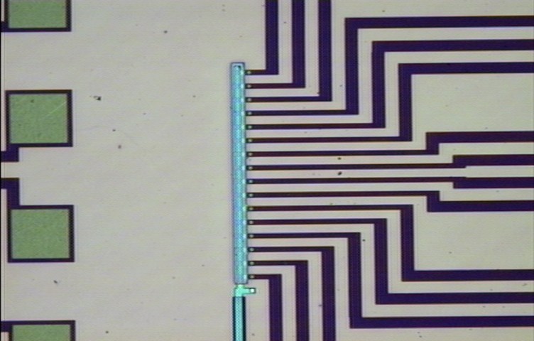
Radiant Technologies has a complete integrated ferroelectric capacitor process running on 5-micron design rules. Capacitors as small as 5µ on a side up to 1 centimeter on a side consisting of 2600Å 20/80 PZT or 1µ 4% niobium-doped 20/80 PZT.
The capacitors are passivated with Radiant's patented interlayer dielectric stack allowing them to be packaged in TO type transistor packages.
A set of design rules and a pre-formatted wafer file in GDS-II format are available upon request.
At some time in the near future Radiant will expand the foundry process to allow the fabrication of piezoelectric cantilevers, membranes, and platforms.
Please contact us with any requests.
